The Hook: Hitting the Glass Ceiling
For 70 years, we have been running on Silicon. It is the workhorse of the solar industry—reliable, cheap, and abundant. It transformed solar from a satellite-only curiosity into the cheapest form of electricity in history. But nature has a speed limit, and Silicon has just about hit it.
The theoretical maximum efficiency of a standard silicon solar cell is defined by the Shockley-Queisser Limit, which sits at roughly 33.7%. In practice, owing to contact resistance, optical losses, and manufacturing defects, commercial panels are stalling out around 24-26%. We are fighting for tenths of a percentage point. Engineers are now scraping the bottom of the barrel, optimizing electrode grids and surface textures to squeeze out one more electron.
But what if we didn’t have to choose just one material? What if the solution wasn’t to make Silicon better, but to give it a partner?
Enter Perovskite. Named after a mineral hidden in the Ural Mountains by Gustav Rose in 1839, this specific crystal structure () is the “Silicon Killer.” Not because it will replace silicon, but because it will ride on top of it.
In 2025, companies like Oxford PV are rolling out “Tandem Cells”—a perovskite layer sprayed on top of a standard silicon wafer. The result? Efficiencies that shatter the Shockley-Queisser limit, pushing toward 30% and beyond in commercial formats.
This isn’t just an upgrade; it is a fundamental shift in the physics of how we harvest light.
The Physics Deep Dive: Why Two Bandgaps Are Better Than One
To understand why Perovskite is a game-changer, you have to look at the Bandgap. This is the amount of energy required to knock an electron loose so it can flow as current.
The Silicon Problem (1.1 eV)
Light comes in a spectrum, from high-energy ultraviolet (UV) and blue light to low-energy infrared (IR).
- Silicon’s Bandgap: ~1.1 eV (Electron Volts).
- The Goldilocks Zone: Silicon is optimized for the red and near-infrared part of the spectrum. It loves photons with about 1.1 to 1.4 eV of energy.
- The Thermalization Loss: When a high-energy blue photon (say, 3.0 eV) hits silicon, it knocks an electron loose, but it has too much energy. That excess energy (1.9 eV) doesn’t become electricity; it is instantly lost as lattice vibrations—heat. It effectively throws away the high-octane fuel. This “Thermalization” is the primary reason why single-junction cells can’t be 100% efficient.
The Tandem Solution: Spectral Splitting
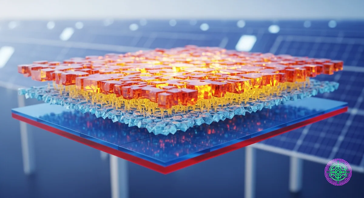
A Tandem Cell stacks two materials with different bandgaps. This is physics engineering at its finest.
- Top Layer (Perovskite): Tuned to a Wide Bandgap (~1.7 eV). This crystal is engineered to be “transparent” to low-energy red/infrared light but greedily absorbs the high-energy blue/green photons. It captures that 3.0 eV photon and converts it efficiently, minimizing the thermalization loss.
- Bottom Layer (Silicon): The red/infrared light passes right through the Perovskite (which looks like yellow tinted glass to these photons) and hits the Silicon layer below. The Silicon then absorbs this lower-energy light exactly as it was designed to.
It is like using a sieve. The top sieve catches the big rocks (Blue Light), and the bottom sieve catches the sand (Red Light). If you only used the bottom sieve, the big rocks would smash through or get stuck. By using both, you capture everything efficiently.
By splitting the spectrum, we stop forcing one material to do a job it’s bad at. The theoretical limit for this “Tandem” approach isn’t 33%—it is over 43%.
Contextual History: From Lab Curiosity to Record Breaker
The story of Perovskite is the fastest development curve in solar history.
- 2009 (The Beginning): Tsutomu Miyasaka at Toin University of Yokohama first used a perovskite material in a solar cell. The efficiency was a measly 3.8%, and the cell dissolved in the liquid electrolyte almost immediately. It was a failure, but an interesting one.
- 2012 (The Solid State): Researchers at Oxford (Henry Snaith) and EPFL (Michael Grätzel) replaced the liquid with a solid hole conductor. Efficiency jumped to 10%. Suddenly, the world paid attention.
- 2013-2020 (The Gold Rush): Thousands of labs pivoted to Perovskite. Efficiencies skyrocketed from 10% to 25% in just seven years. For context, it took Silicon 40 years to make that same climb.
- 2024 (The Commercial Era): Oxford PV finally broke the “Lab” barrier, certifying commercial-sized cells at 28.6%.
This meteoric rise is due to the structure of the crystal itself. Perovskites are “defect tolerant.” In silicon, a single impurity can kill the cell. In perovskite, the electrons can essentially dodge the defects, meaning you don’t need the hyper-pure, expensive manufacturing environments required for silicon.
The Manufacturing Revolution: Printing vs. Melting
One of the most overlooked aspects of this technology is the Energy Payback Time (EPBT).
The Old Way: Czochralski Process
Making a silicon panel is energy-intensive.
- You mine quartz (SiO2).
- You blast it in an arc furnace to get Metallurgical Grade Silicon.
- You purify it into Polysilicon.
- You melt it at 1,400°C in a crucible and slowly pull out a single giant crystal (The Czochralski method).
- You saw that crystal into wafers, wasting 40% of the material as “kerf” (dust). This massive energy input means a silicon panel has to run for 1-2 years just to “pay back” the energy used to make it.
The New Way: Solution Processing
Perovskites are made via Solution Processing.
- You mix precursor chemicals (Lead Iodide, Organic Salts) in a solvent (like ink).
- You put your silicon wafer on a conveyor belt.
- You print the perovskite ink onto the wafer using a slot-die coater (like a high-tech newspaper printer) or evaporate it in a vacuum chamber.
- You bake it at a measly 100-150°C to crystallize it.
The energy input is a fraction of silicon’s. This means Perovskite tandems could eventually have a lower carbon footprint and a faster energy payback time (<6 months), even with the added complexity of a second layer.
The Commercial Breakthrough: Oxford PV
For a decade, Perovskite was a “lab queen”—impressive in a controlled environment, but useless in the real world. Why? Because it dissolved.
Early perovskite crystals were notoriously unstable. They would degrade in hours when exposed to:
- Moisture: Water molecules would penetrate the crystal lattice, causing it to revert to lead iodide (turning from black to yellow).
- Oxygen: combined with light would create superoxides that ate the material.
- Heat: Rooftops get hot. Early formulas broke down at 60°C.
The 2024-2025 Turnaround
Oxford PV, a spin-out from the University of Oxford, solved this not by changing the physics, but by mastering the Encapsulation and Composition.
- Commercial Record: In 2024, they certified a 26.9% efficiency on a commercial-sized module (60 cells). Compare that to the standard 22-23% top-tier silicon panel you can buy today.
- Deployment: As of late 2024 and throughout 2025, the first commercial shipments have started landing. They aren’t just selling cells; they are selling the future of the grid.
Their secret sauce? A proprietary perovskite formulation that replaces the unstable Methylammonium usually found in lab cells with more robust cations like Formamidinium and Cesium, heavily doped with additives that “passivate” (heal) defects in the crystal structure.
The Stability Challenge: “The Rain Test”
The biggest criticism of Perovskite has always been longevity. A silicon panel lasts 25 years. Can a crystal grown from solution do the same?
Market-ready Perovskites are now passing the IEC 61215 standard—the “torture test” for solar panels, involving:
- Damp Heat: 1,000 hours at 85°C and 85% humidity.
- Thermal Cycling: freezing to -40°C and heating to 85°C hundreds of times.
The latest research indicates that with Atomic Layer Deposition (ALD) encapsulation—wrapping the cell in a layer of glass or polymer only a few atoms thick—we can seal out moisture completely. The result is a panel that degrades at roughly the same rate as silicon (<0.5% per year).
Forward-Looking Analysis: 2026 and Beyond
We are in the “Early Adopter” phase of the S-curve.
- Cost: Currently, Tandem cells are more expensive to manufacture because they require extra processing steps (adding the Perovskite layer). The Levelized Cost of Electricity (LCOE) is slightly higher than commodity silicon, but the value proposition is the Density.
- The “Premium” Market: Expect to see these first on space-constrained rooftops, luxury EVs (like the Mercedes Vision EQXX concept), and satellites, where W/m² matters more than $/W.
By 2030, analysts predict “Pure Silicon” panels will become the budget option, while “Tandem Perovskite” becomes the industry standard. The rooftop of the future won’t just be blue; it will be a shimmering, multi-layered engine of quantum efficiency.
The Silicon Era isn’t over, but it has found its partner. And together, they are finally harvesting the full power of the sun.


🦋 Discussion on Bluesky
Discuss on Bluesky